PTF141501E
Thermally-Enhanced High Power RF LDMOS FET
150 W, 1450 – 1500 MHz, 1600 – 1700 MHz
Description
The PTF141501E is a 150-watt, GOLDMOS ® FET intended for DAB
applications. This device is characterized for Digital Audio Broadcast
operation in the 1450 to 1500 MHz band. Thermally-enhanced packaging
provides the coolest operation available. Full gold metallization ensures
excellent device lifetime and reliability.
Features
DAB Drive-up at 28 Volts
35
-20
30
-25
-30
Regrowth
20
-35
Efficiency
15
-40
10
-45
5
-50
Spectral Regrowth (dBc)
Drain Efficiency (%)
VDD = 28 V, f = 1500 MHz, IDQ = 1.5 A, DAB mode 2
25
PTF141501E
Package H-30260-2
•
Thermally-enhanced package, pB-free and
RoHS-compliant
•
Broadband internal matching
•
Typical DAB Mode 2 performance at 1500
MHz, 32 V
- Average output power = 50 W
- Efficiency = 28%
- Spectral regrowth = –30 dBc
- ∆ 975 kHz fC
•
Typical DAB Mode 2 performance at 1500
MHz, 28 V
- Average output power = 40 W
- Efficiency = 26%
- Spectral regrowth = –31 dBc
- ∆ 975 kHz fC
•
Typical CW performance, 1500 MHz, 28 V
- Minimum output power = 150 W
- Linear gain = 16.5 dB
- Efficiency = 48% at P–1dB
•
Integrated ESD protection: Human Body
Model, Class 1 (minimum)
•
Excellent thermal stability, low HCI drift
•
Capable of handling 10:1 VSWR at 28 V, 150
W (CW) output power
-55
0
0
10
20
30
40
50
60
Output Power (W) Average
RF Characteristics
DAB Measurements (not subject to production test—verified by design/characterization in Infineon test fixture)
VDD = 32 V, IDQ = 1.5 A, POUT = 50 WAVG, f = 1500 MHz, DAB Mode 2, fC ∆ 975 kHz
Characteristic
Symbol
Min
Typ
Max
Unit
RGTH
—
–30
—
dBc
Gain
Gps
—
16.5
—
dB
Drain Efficiency
ηD
—
29
—
%
Spectral Regrowth
All published data at TCASE = 25°C unless otherwise indicated
*See Infineon distributor for future availability.
ESD: Electrostatic discharge sensitive device—observe handling precautions!
Data Sheet
1 of 12
Rev. 04, 2008-02-13
�PTF141501E
RF Characteristics (cont.)
Two-Tone Measurements (tested in Infineon test fixture)
VDD = 28 V, IDQ = 1.5 A, POUT = 150 WPEP, f = 1500 MHz, tone spacing = 1 MHz
Characteristic
Symbol
Min
Typ
Max
Unit
Gain
Gps
15.0
16.5
—
dB
Drain Efficiency
ηD
35
—
—
%
Intermodulation Distortion
IMD
—
–30
–28
dBc
DC Characteristics
Characteristic
Conditions
Symbol
Min
Typ
Max
Unit
Drain-Source Breakdown Voltage
VGS = 0 V, ID = 10 µA
V(BR)DSS
65
—
—
V
Drain Leakage Current
VDS = 28 V, V GS = 0 V
IDSS
—
—
1.0
µA
On-State Resistance
VGS = 10 V, V DS = 0.1 V
RDS(on)
—
0.07
—
Ω
Operating Gate Voltage
VDS = 28 V, IDQ = 1.5 A
VGS
2.5
3.3
4.0
V
Gate Leakage Current
VGS = +10 V, V DS = 0 V
IGSS
—
—
1.0
µA
Maximum Ratings
Parameter
Symbol
Value
Unit
Drain-Source Voltage
VDSS
65
V
Gate-Source Voltage
VGS
–0.5 to +12
V
Junction Temperature
TJ
200
°C
Total Device Dissipation
PD
438
W
2.5
W/°C
Above 25°C derate by
Storage Temperature Range
TSTG
–40 to +150
°C
Thermal Resistance (TCASE = 70°C)
RθJC
0.4
°C/W
Ordering Information
Type
Package Outline
Package Description
Marking
PTF141501E
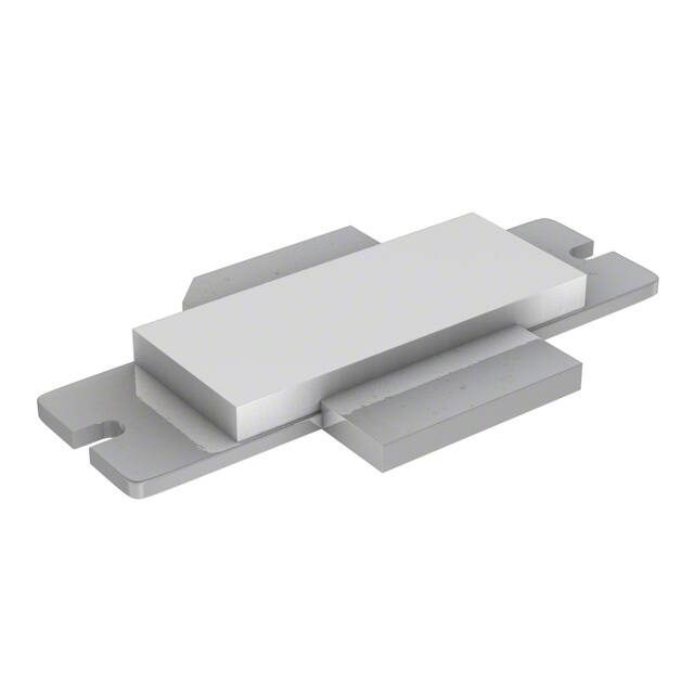
H-30260-2
Thermally-enhanced slotted flange, single-ended
PTF141501E
*See Infineon distributor for future availability.
Data Sheet
2 of 12
Rev. 04, 2008-02-13
�PTF141501E
CW Sweep in a Broadband Test Fixture
VDD = 28 V, IDQ = 1.5 A, POUT (CW) = 30 W
-20
30
-25
25
-30
Efficiency
-35
Regrowth
15
-40
10
-45
5
-50
-55
0
0
10
20
30
40
50
60
Drain Efficiency
25
-5
20
-10
15
-15
Gain
10
-20
Return Loss
-25
5
0
1400
1450
1500
-30
1600
1550
Output Power (W) Average
Frequency (MHZ)
CW Sweep
for Varying Bias Conditions
Intermodulation Distortion Products
vs. Output Power
VDD = 28 V, f = 1500 MHz
VDD = 28, IDQ = 1.5 A, f = 1.5 GHz, tone spacing = 1 MHz
17
Intermodulation Distortion (dBc)
-25
IDQ = 1.5 A
Gain (dB)
0
IDQ = 1.2 A
16
IDQ = 0.9 A
IDQ = 0.6 A
15
14
1
10
100
-30
-35
35
Drain Efficiency
-40
1000
IM5
-45
25
-50
-55
15
IM7
-60
-65
0
20
40
60
80
5
100
Output Power (W) Average
Output Power (W) CW
Data Sheet
45
IM3
Drain Efficiency (%) .
20
30
Input Return Loss (dB)
35
Gain (dB) and Drain Efficiency (%) .
DAB Drive-up at 32 Volts
VDD = 32, IDQ = 1.5 A, f = 1500 MHz, DAB Mode 2
Spectral Regrowth (dBc)
Drain Efficiency (%) .
Typical Performance
3 of 12
Rev. 04, 2008-02-13
�PTF141501E
Typical Performance (cont.)
Intermodulation Distortion vs. Output Power
for Various I DQ
Bias Voltage vs. Temperature
Voltage normalized to typical gate voltage.
Series show current.
VDD = 28, f = 1.5 GHz
-25
-30
Normalized Bias Voltage
IDQ = 1.1 A
IM3 (dBc)
-35
-40
-45
IDQ = 1.3 A
-50
IDQ = 1.5 A
-55
-60
IDQ = 1.7 A
-65
IDQ = 1.9 A
-70
0
50
100
1.04
0.90 A
1.03
2.10 A
1.02
4.50 A
1.01
7.50 A
1.00
10.50 A
0.99
13.50 A
0.98
0.97
0.96
0.95
-20
150
0
Output Power (W) Average
20
40
60
80
100
Case Temperature (ºC)
D GE
NE
Broadband Circuit Impedance, 1500 MHz
D
Z Source
Z0 = 50 Ω
Z Load
0.1
Z Load
1600 MHz
R
jX
R
jX
1400
5.00
–6.70
0.94
1.27
1450
4.50
–5.90
0.90
1.73
1500
4.20
–5.10
0.86
2.21
1550
3.90
–4.30
0.82
2.60
1600
3.70
–3.70
0.80
3.05
Data Sheet
4 of 12
0.2
1400 MHz
Z Source
1600 MHz
0.1
1400 MHz
---
MHz
D LOA D S T OW AR
NGT H
Z Load Ω
ELE
WAV
Z Source Ω
Frequency
0 .0
S
0.1
G
Rev. 04, 2008-02-13
�PTF141501E
Reference Circuit for 1500 MHz
C1
0.001µF
R2
1.3K V
R1
1.2K V
QQ1
LM7805
Q1
VDD
Q1
BCP56
C2
0.001µF
R3
2K V
C3
0.001µF
R4
2K V
R5
5.1K V
C4
10µF
35V
R6
10 V
C5
0.1µF
L1
R7
5.1K V
C10
13pF
C6
7.5pF
l6
l1
C12
0.1µF
C19
33pF
DUT
l2
V DD
C13
10µF
35V
l7
C7
33pF
RF_IN
C11
1µF
l3
l4
C8
0.3pF
C9
2.4pF
l5
l9
l10
l11
l12
l13
C18
0.7pF
l8
l14
RF_OUT
C20
0.3pF
L2
C14
13pF
C15
1µF
C16
0.1µF
C17
10µF
35V
141501a-1500_sch
Reference Circuit Schematic for 1500 MHz
Circuit Assembly Information
DUT
PTF141501E
PCB
0.76 mm [0.030"] thick, εr = 4.5
Microstrip
l1
l2
l3
l4
l5
l6
l7
l8
l9
l10
l11
l12
l13
l14
LDMOS Transistor
TMM4
Electrical Characteristics at 1500 MHz 1 Dimensions: L x W (mm)
0.043 λ, 50.0 Ω
4.67 x 1.47
0.118 λ, 42.0 Ω
12.70 x 1.85
0.015 λ, 42.0 Ω
1.57 x 1.85
0.012 λ, 14.7 Ω
1.22 x 7.57
0.052 λ, 8.0 Ω
5.08 x 15.19
0.182 λ, 60.0 Ω
20.17 x 0.97
0.283 λ, 63.0 Ω
31.45 x 0.89
0.283 λ, 63.0 Ω
31.45 x 0.89
0.026 λ, 4.6 Ω
2.46 x 27.89
0.086 λ, 4.6 Ω
8.23 x 27.89
0.061 λ, 9.4 Ω
5.97 x 12.62
0.011 λ, 50.0 Ω
1.14 x 1.47
0.056 λ, 50.0 Ω
6.10 x 1.47
0.010 λ, 50.0 Ω
1.07 x 1.47
2 oz. copper, both sides
Dimensions: L x W (in.)
0.185 x 0.058
0.500 x 0.073
0.062 x 0.073
0.048 x 0.298
0.200 x 0.598
0.794 x 0.038
1.238 x 0.035
1.238 x 0.035
0.097 x 1.098
0.324 x 1.098
0.235 x 0.497
0.045 x 0.058
0.240 x 0.058
0.042 x 0.058
1Electrical Characteristics are rounded.
Data Sheet
5 of 12
Rev. 04, 2008-02-13
�PTF141501E
Reference Circuit for 1500 MHz (cont.)
R5 C5 R4 R3 C3 C1
10
35V
R2
LM
QQ1
C2
C10
C11
R6 C6 R7
L1
Q1
10
35V
+
R1
C12
R5 C5 R4 R3 C3 C1
C13
RF_OUT
C16
C8
C9
C17
C18
VDD
C20
C19
C7
VDD
VDD
C4
10
+
35V
R2
LM
QQ1
C2
+
RF_IN
+
C4
VDD
R6 C6 R7
L2
10
35V
C15
C14
R1
Q1
141501ef-1500_dtl
141501ef-1500_assy
Reference circuit (not to scale)*
Component
C1, C2, C3
C4, C13, C17
C5, C12, C16
C6
C7
C8
C9
C10, C14
C11, C15
C18
C19
C20
L1, L2
Q1
QQ1
R1
R2
R3
R4
R5, R7
R6
Description
Capacitor, 0.001 µF, 50 V, 0603
Capacitor, 10 µF, 35 V, SMD
Capacitor, 0.1 µF, 50 V, 1206
Capacitor, 7.5 pF
Capacitor, 33 pF
Capacitor, 0.3 pF
Capacitor, 2.4 pF
Capacitor, 13 pF
Capacitor, 1 µF, 50 V
Capacitor, 0.7 pF
Capacitor, 33 pF
Capacitor, 0.3 pF
Ferrite, 6 mm
Transistor
Voltage regulator
Resistor, 1.2 k-ohms, 1/10 W, 0603
Resistor, 1.3 k-ohms, 1/10 W, 0603
Resistor, 2 k-ohms, 1/10 W, 0603
Potentiometer, 2 k-ohms, 0.25 W
Resistor, 5.1 k-ohms, 1/4 W, 1206
Resistor, 10 ohms, 1/4 W, 1206
Suggested Manufacturer
Digi-Key
Digi-Key
Digi-Key
ATC
ATC
ATC
ATC
ATC
Digi-Key
ATC
ATC
ATC
Philips
Infineon
Digi-Key
Digi-Key
Digi-Key
Digi-Key
Digi-Key
Digi-Key
Digi-Key
P/N or Comment
PCC1772CT-ND
PCS6106TR-ND, Tant. TE Series
P4525-ND
100A 7R5
100A 330
100A 0R3
100A 2R4
100B 130
19528-ND
100B 0R7
100B 330
100B 0R3
53/3/4.6-452
BCP56
LM7805
P1.2KGCT-ND
P1.3KGCT-ND
P2KGCT-ND
3224W-202ETR-ND
P5.1KECT-ND
P10ECT-ND
*Gerber files for this circuit are available on request.
Data Sheet
6 of 12
Rev. 04, 2008-02-13
�PTF141501E
Alternate Application for 1600 MHz
Typical Performance
Frequency Sweep, 1.6 – 1.7 GHz
CW Power Sweep
(1600 MHz application circuit)
VDD = 28 V, IDQ = 1.2 A
VDD = 28 V, IDQ = 1.2 A, f = 1675 MHz
50
Gain (dB)
Gain
30
15
20
14
Efficiency
13
0
20
40
60
10
16
Gain (dB)
40
16
17
Drain Efficiency (%)
17
15
14
0
80 100 120 140 160 180
13
1580 1600 1620 1640 1660 1680 1700 1720
Output Power (W)
Frequency (MHz)
2-Tone Drive-up at Optimum Current
VDD = 28 V, IDQ = 1.2 A, f1 = 1675 MHz, f2 = 1676 MHz
0
35
-10
Efficiency
IMD (dBc)
-20
30
25
-30
20
3rd Order
-40
15
5th
7th
-50
-60
10
5
-70
0
20
40
60
80
0
100
Output Power (W) Average
Data Sheet
7 of 12
Rev. 04, 2008-02-13
�PTF141501E
Broadband Circuit Impedance, 1600 MHz
Z Source Ω
Frequency
0.1
0.0
D LOA D S T OW AR
jX
1600
9.5
–5.6
0.9
–5.8
1625
9.6
–5.2
0.8
–5.4
1650
9.8
–5.0
0.8
–5.2
1675
9.9
–4.7
0.8
–5.0
1700
10.0
–4.4
0.8
–4.8
Z0 = 50 Ω
Z Source
Z Load
NGT H
- W AV
S
R
0.5
G
jX
0.4
Z Load
R
0.3
Z Source
Z Load Ω
MHz
0.2
D
1700 MHz
1600 MHz
1600 MHz